描述
Key Features & Improvements over M57962L
It retains all the critical features of the M57962L but with enhancements:
Integrated VCE(sat) Desaturation Detection: This is the primary protection feature. It monitors the voltage across the IGBT’s Collector and Emitter (VCE) during the “on” state.
How it works: If the IGBT goes into a short-circuit or overcurrent condition, the VCE voltage will rise sharply (a state called “desaturation”).
The driver detects this voltage rise and immediately initiates a soft, controlled turn-off to protect the IGBT from destructive thermal runaway.
Improved Undervoltage Lockout (UVLO): Monitors both the positive (+Vcc) and negative (-Vee) gate drive supply voltages. If either supply drops below a safe threshold, the UVLO circuit blocks the input signal and ensures the IGBT remains off, preventing it from operating in its linear region (which causes excessive heat).
High Input-Output Isolation: Provides galvanic isolation (typically 2500 Vrms) between the low-voltage control circuit and the high-voltage power stage, which is crucial for safety and noise immunity.
High Output Current: Capable of delivering high peak gate currents (e.g., +2.5A for turn-on and -5.0A for turn-off), enabling fast switching of large IGBT modules and minimizing switching losses.
Built-in “Soft” Shut-down: Upon detecting a fault, it doesn’t just cut the gate signal; it gradually reduces the gate voltage to slow down the turn-off. This “soft” shutdown prevents a dangerously high dv/dt from causing voltage spikes that could destroy the IGBT.
Typical Applications
This driver is used in high-power, high-reliability industrial systems, including:
High-Power Motor Drives & AC Servo Drives
Uninterruptible Power Supplies (UPS)
Industrial Inverters & Converters
Power Supplies for Welding and Heating
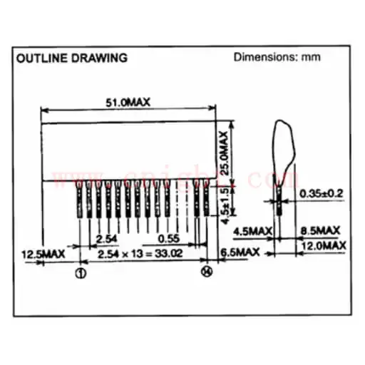
Pin Configuration (Standard SIL Package)
The module is typically in a single-in-line (SIL) package. The exact pinout should always be verified with the official datasheet, but a common configuration is:
Control Side (Input):
Pin 13, 14: Signal Input (In+, In- for differential operation).
Pin 1, 2: Control Ground (GND1).
Power Side (Output – Connects to IGBT):
Pin 6, 7: Gate Drive Output (G) -> Connects to IGBT gate.
Pin 8: Desaturation Detection Input (C) -> Connects to IGBT collector via a high-voltage fast-recovery diode.
Pin 9, 10: Power Return / Emitter (E) -> Connects to IGBT emitter.
Pin 3, 4, 5: Positive Gate Supply Voltage (Vcc, e.g., +15V).
Pin 11, 12: Negative Gate Supply Voltage (Vee, e.g., -10V).
Key Electrical Characteristics (Summary)
Parameter Symbol Typical Value Unit
Supply Voltage (Vcc) Vcc +15 to +18 V
Supply Voltage (Vee) Vee -10 to -15 V
Peak Output Current (Source) IOH +2.5 A
Peak Output Current (Sink) IOL -5.0 A
Input Threshold Voltage (High) VIH ~3.5 V
Isolation Voltage Viso 2500 Vrms
Propagation Delay tPLH, tPHL ~1.0 ¦Ìs